Nanotechnology
Abstract
This article provides an introduction to nanotechnology as well as some of the benefits and challenges surrounding the field. In particular, it discusses the desirability of nanomaterials leading to its promising usability in nanodevices. On the other side of the discussion is a look into some risks and challenges that come from working with nanodevices.
Overview
Research and development in nanotechnology has been and still is an area of high interest that continues to be highly funded. Part of this is due to the promising nature of the many applications and disciplines that nanotechnology encompasses. Some areas where nanotechnology is applicable include biotechnology, chemical engineering, physics, and electrical engineering. However, the development of nanodevices is rarely true to just one of these areas; instead it is interdisciplinary. For this article, the focus will be centered around nanotechnology within the electrical engineering realm, and in particular, the benefits and desirability of nanotechnology as well as the ethics, risks, and challenges commonly faced with nanodevices.
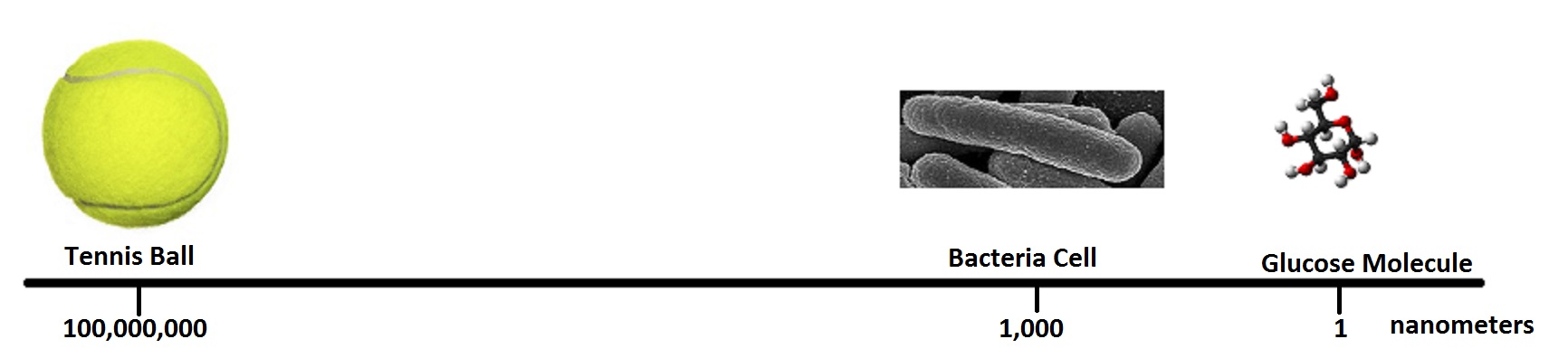
Before all these topics can be approached, let’s look at what nanotechnology really is. First, we have to get an understanding of the size of one nanometer. From Figure 1, we can see that a tennis ball, something we can easily cup in our hands, is 100 million nanometers in diameter. If we divided the length of that into 100 thousand pieces, the result would be the size of a bacteria cell. To look at a bacteria cell, we already need a high-powered microscope. In order to get one nanometer, approximately the size of a glucose molecule, we need to slice a bacteria-sized particle a thousand more times. In order to see a particle that small, we already need sophisticated methods such as electron microscopy. So to actually generate usable materials and devices is, of course, much more difficult, but particular properties of nano-particles make them desirable enough for such difficulties.
Desirability
From chemistry classes in high school, we have heard of atoms and molecules and the elements on the periodic table. We have likely sat through at least a lecture or two on chemical reactions and molecules binding to form materials such as our DNA, metals, and other everyday objects. But while we learn about basic chemical structures that were discovered decades and even hundreds of years ago, modern research continues toward unprecedented discoveries in molecules and particles on the nanometer scale.
Nanoparticles continue to be interesting to scientists because of the chemical and physical properties that come from synthesizing such small particles. For example, chemists and biologists construct nanoparticles to take on desired structures so that they will bind to damaging molecules in diseased patients. Similar ideas are taken into constructing semiconductors, since electrical characteristics are altered when the size of semiconductors are greatly reduced. The quantum dot, for example, uses semiconducting materials to form a nanocrystal which can be used to develop transistors, diodes, lasers, and solar cells (Lacaze, 2012, pp. 54-58). Aside from its semi-conducting properties, quantum dots are particularly interesting because of their fluorescence. The color that is produced from the nanocrystal depends on its size which alters the light that is emitted. One application that emerged from quantum dots is the Sony TV that incorporates technology from QD Vision to make more colorful Sony TVs (Bullis, 2013).
Expanding into larger nanomaterials, nanowires, which are a few nanometers in diameter and a few micrometers long, are the basis for making small electrical devices. Since 1991, interest and research in nanowires have been growing exponentially (Lacaze, 2012, pp. 60-62). These nanowires are silicon-based but have electrical properties that are much different from larger silicon parts, and give rise to certain types of nanotransistors. One type is the field effect transistor, which is used in practically every electrical device and paves the path for increasingly small devices.
The capability to reduce the size of electronic devices and the parts used to make such devices ties into Moore’s Law (Figure 2), which is an observational view on the desirability of small circuits. Moore’s Law theorizes that the number of transistors on an integrated circuit exponentially increases by doubling the number of transistors every two years.
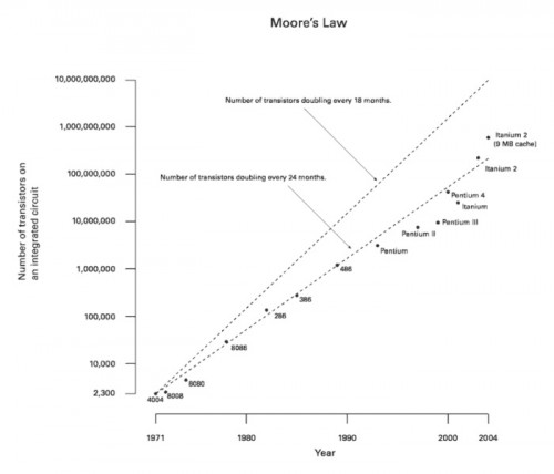
Although the law can’t remain true forever since systems are still bound by the laws of physics, the possibility of nanodevices continues to drive the theory for now.
In addition to increasing the number of transistors on an integrated circuit, the other value to making transistors smaller is less energy consumption. Since data storage is so cheap. the amount of data available continues to increase, which ultimately leads to high energy consumption by large servers. In a report from the International Data Corporation (IDC), the amount of digital information increased by a factor of 10 from 2006 to 2011 (Lacaze, 2012, pp. 123). While it is easy to obtain more storage for all the data, managing data and data traffic results in higher energy use in servers.
Challenges of Fabrication
Part of the growing trend in nanotechnology research is because the development of one nanotechnology often leads to a need for another nanotechnology. For example, to build scaled-down integrated circuits, there needs to also be scaled down interconnects to communicate between devices. The need for such interconnects fueled the research of nanowires and carbon nanotubes. Carbon nanotubes are another possible interconnect for nanodevices that are lightweight, durable and extremely conductive.
Perhaps, the most difficult part of developing a product is the integration of all the necessary parts. While there may be research to develop nanoscale interconnnects and transistors, there needs to be a practical way to piece those parts on an integrated circuit that runs efficiently. But as mentioned before, even viewing on the nanoscale is difficult, and as such, fabrication of such small integrated circuits is even more so. However, even after developing these products, there still needs to be research to continue to improve them, and also to develop large-scale manufacturing techniques for such products.
Currently integrated circuits are fabricated using lithography, which uses light to imprint the desired integrated circuit pattern onto a silicon wafer, a thin piece of crystalline silicon that serves as a base for the integrated circuit. In this process, the resolution of the pattern is limited to the wavelengths of the light used. As a result, in order to fabricate smaller circuits, it is important to construct shorter wavelengths of light. To develop a 32nm wavelength, Intel used refraction techniques to decrease a wavelength by about 30 percent. In order to go below that, possible solutions exist including extreme ultraviolet (EUV) lithography and a process of “double patterning” (Freebody, 2011). However, even with such proposed techniques, the industry still struggles with wavelengths below 32nm since both EUV and “double patterning” aren’t easily implemented. To implement EUV at a large scale, a powerful source is needed, but even today, we are nowhere near finding a powerful enough source. In addition, both of those techniques are costly and would not be ideal for large scale industry needs.
Public Impact
While low cost, efficiency and Moore’s Law may be important to industry, the rise of nanotechnology also beckons for public consideration and safety. As so much of today’s work is poured into new discoveries in technology, the number of new technologies coming out is increasingly fast. They are surrounding new generations in many aspects of home and social life, and are only sparingly integrated into the classroom experience. In one part, technology can be a distraction for learning, but in another respect, in order for future generations to continue to improve technology, they first have to be familiar with technology that already exists. In addition, our educational system is structured very similarly to how it has been for a very long time. But while the information around us gets increasingly complex, the educational infrastructure hasn’t and can’t really have much change. So if the information coming out continues to surpass those who are being affected by it, there will be problems to follow.
One of the more prominent effects is regulation. As technologies become so small that they can affect the binding of molecules in a human body, they need to be considered as a chemical and regulated like so. There have already been some cases where devices containing nanoparticles or nanotechnology parts have had harmful effects (Ramsden, 2011, 12.6.2), yet there has been little change in regulation. From looking at the Food and Drug Administration (FDA) itself, there are already cases where additives of foods once cleared later aren’t usable after more research. Although the FDA is highly scrupulous and very good with the majority of what they do for the public, it is important to acknowledge that there are always errors. More importantly though, in a society where decisions are just bounded by the law and businesses are looking to thrive, there are always loopholes and many businesses will be looking for them.
Some of what has been mentioned in this section comes from personal opinions, and it may seem that these opinions are not the best. But these are not just one person’s opinions and they are not opinions that have been formed on a whim. There are reasons why these opinions exist, and as a result, there is a public distrust that is present when it comes to regulation. Because of this, it is important to implement better risk research to hopefully improve regulation. While nanotechnology is still new, “getting nanotechnology right the first time” (Hunt, 2006, 3.11) is important so public distrust doesn’t continue to form. For something that is still climbing its way up the ladder, there is still a lot of research to be done, improvements to be made, and regulations and changes to be considered. However, for now, unless we are one of the people with the education and power to do one of these tasks, all we can do is to keep ourselves informed and prepared.
Conclusion
From this article alone, it is apparent that there is a lot of information already surrounding nanotechnology, even though there is still a lot to be learned. As mentioned in the introduction, the research to guide nanotechnology is interdisciplinary, although many of the topics mentioned in this article are focused around electrical engineering concepts. The reason for this is that electrical engineering is an integral part of nanotechnology research. From transistors to semiconductors to integrated circuits, the basis of electrical engineering is also the basis for nanotechnology.
Bibliography
- Bullis, K. (n.d.). Quantum Dots Get Commercial Debut in More Colorful Sony TVs. Retrieved from http://www.technologyreview.com/news/509801/quantum-dots-get-commercial-debut-in-more-colorful-sony-tvs/
- Freebody, M. (n.d.). Preserving Moore’s Law Pushes Lithography to its Limits. Retrieved from http://www.photonics.com/Article.aspx?AID=46862
- Hunt, G. (2006). The Global Ethics of Nanotechnology. In Hunt, G., & Mehta, M. D. (Eds.), Nanotechnology: Risk, ethics and law. London: Earthscan. OCLC WorldCat Permalink: http://www.worldcat.org/oclc/62878715
- Lacaze, P. (2013). Nanotechnologies: Concepts, processing and applications. London; Hoboken, N.J: ISTE. OCLC WorldCat Permalink: http://www.worldcat.org/oclc/822214899
- Ramsden, J. (2011). Nanotechnology: An introduction. Norwich, N.Y; Oxford: William Andrew. OCLC WorldCat Permalink: http://www.worldcat.org/oclc/744634333
Suggested Reading
- Food and Drug Administration Recalls: http://www.fda.gov/Safety/Recalls/
- About the International Data Corporation: http://www.idc.com/about/about.jsp